Resistor
1. Overview
In this example project, a simple uniformly doped n-type silicon resistor is modelled and simulated to demonstrate the basic workflow of semiconductor device simulation. An analytical resistance is calculated from fundamental semiconductor relations based on geometry, doping concentration, and mobility. The simulation includes geometry definition, doping profile assignment, physical model selection, contact specification, and bias application. The extracted current is used to compute the simulated resistance, and the result is compared with the analytical expectation. This example serves both as a simple validation case for the Aquarius TCAD environment and as an instructional reference for users implementing basic electrical simulations of passive devices.
2. Parameters
| Parameter | Symbol | Value | Unit | Description |
|---|---|---|---|---|
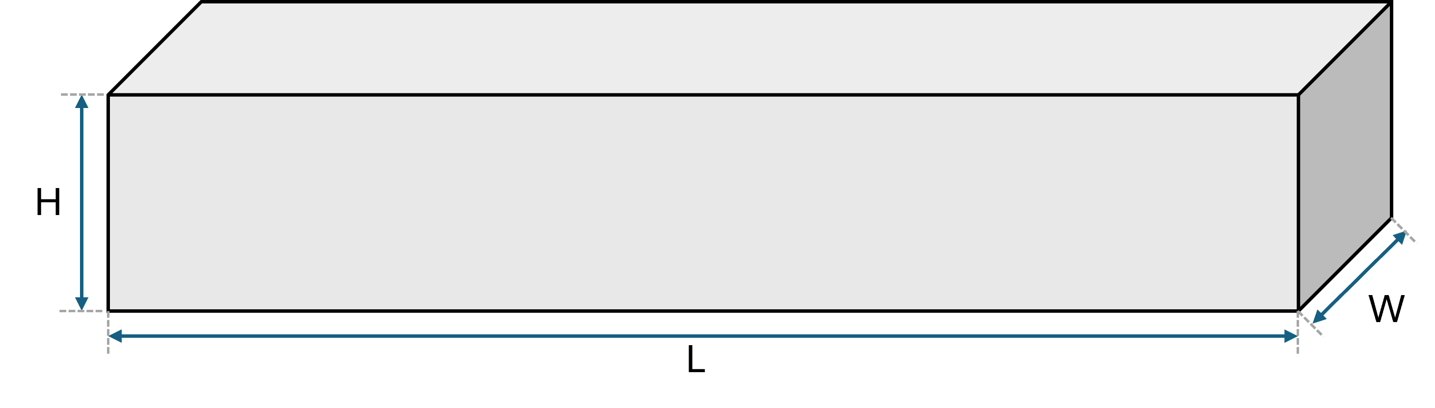
| Length | cm | Distance between the two contacts. | ||
| Width | cm | Width of the resistor. | ||
| Depth | cm | Depth of the resistor. | ||
| Doping Concentration | cm | Uniform donor concentration. | ||
| Carrier Mobility | 1000 | cm/V·s | Nominal electron mobility (constant). |
3. Analytical Result
3.1. Resistance Formula
The analytical resistance of a uniformly doped semiconductor resistor can be derived from Ohm’s law and the definition of resistivity in terms of semiconductor transport properties. The total resistance between two terminals of a rectangular resistor is given by:
Where:
- = resistance (Ω)
- = resistivity of doped silicon (Ω·cm)
- = length of the resistor (cm)
- = cross-sectional area = Height × Depth (cm²)
In a doped semiconductor, the resistivity is related to the doping concentration and carrier mobility as follows:
Where:
- = elementary charge ( C)
- = carrier mobility (cm²/V·s)
- = doping concentration (cm⁻³)
Combining the two equations, the resistance becomes:
3.2. Example Calculation
Using the parameter values defined above:
Now substitute into the resistance formula:
4. Simulation using Aquarius
4.1. Creating the Device Model
To create a resistor device model in Aquarius, follow the steps below.
4.1.1. Launch the Device Editor
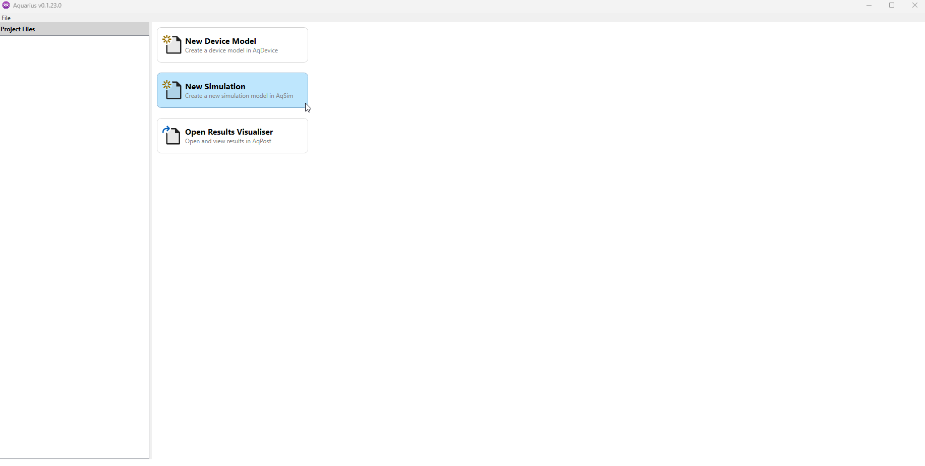
- Open the Aquarius application.
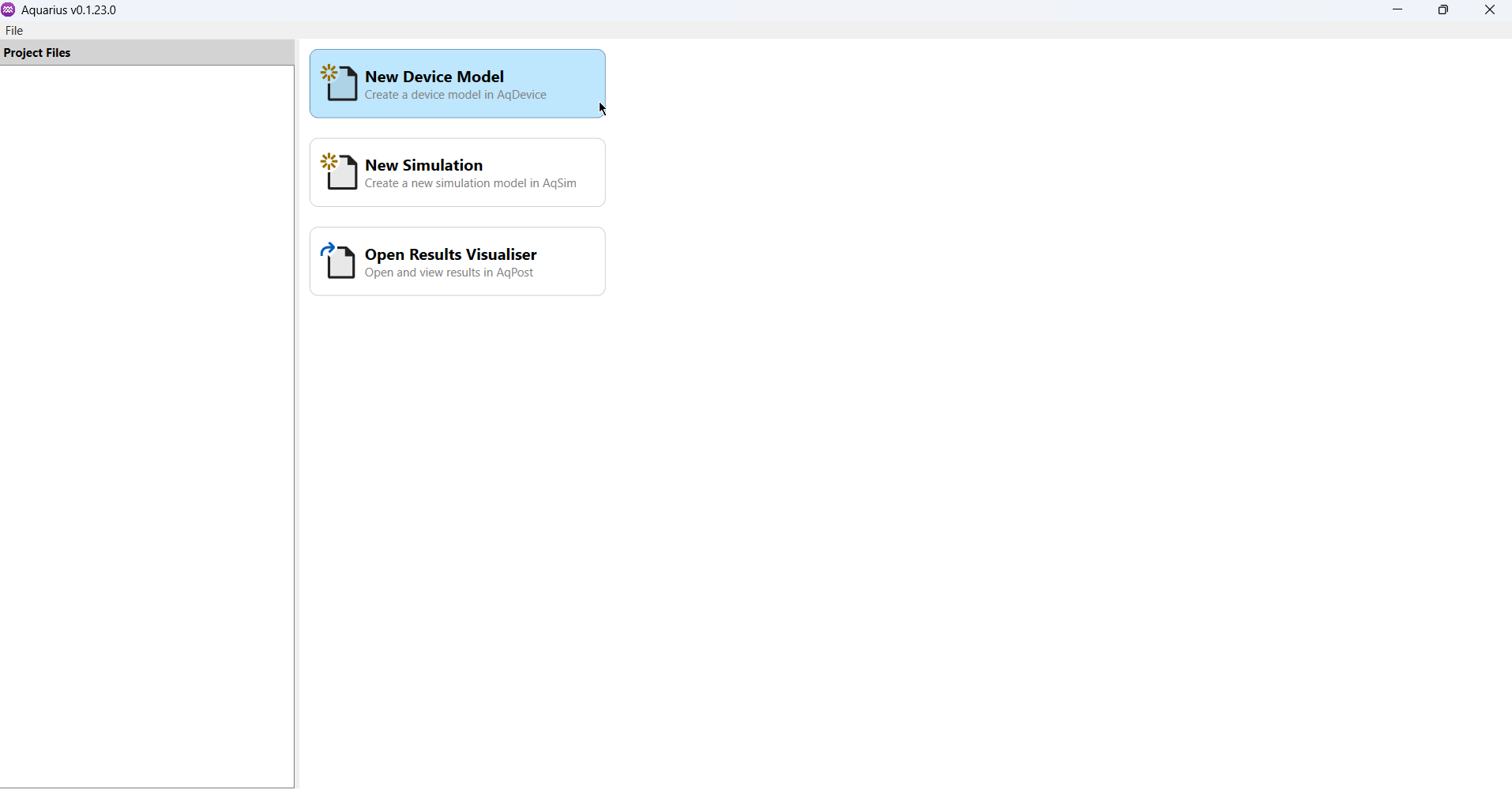
- On the Start Page, three options are available:
- New Device Model
- New Simulation
- Open Results Visualiser
- Click
New Device Model(the first option). - The Device Editor will open with an empty workspace.
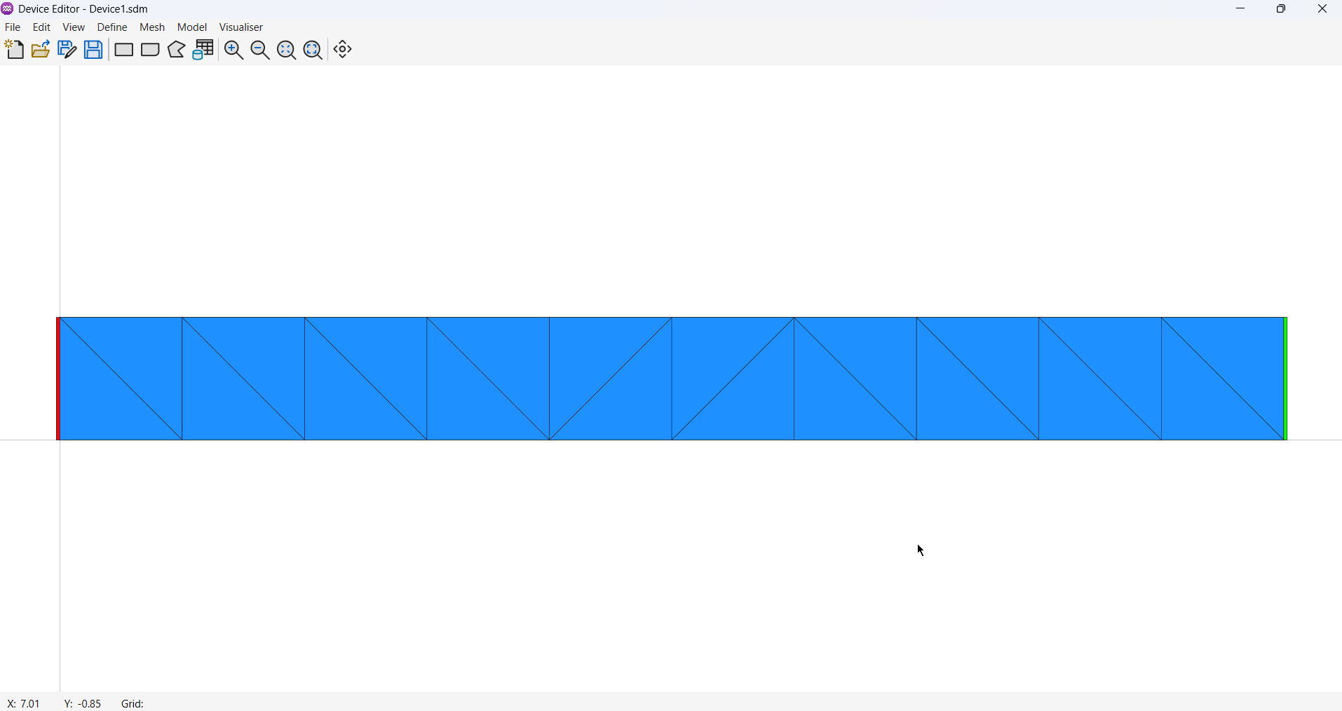
4.1.2. Define the Device Geometry
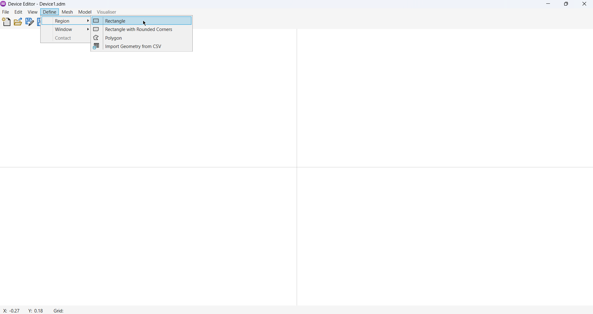
- In the Menu Bar, select
Define→Region→Rectangle.
- Position the cursor on the canvas to draw a rectangular shape:
- Left-click to start drawing.
- Left-click again to finish the shape.
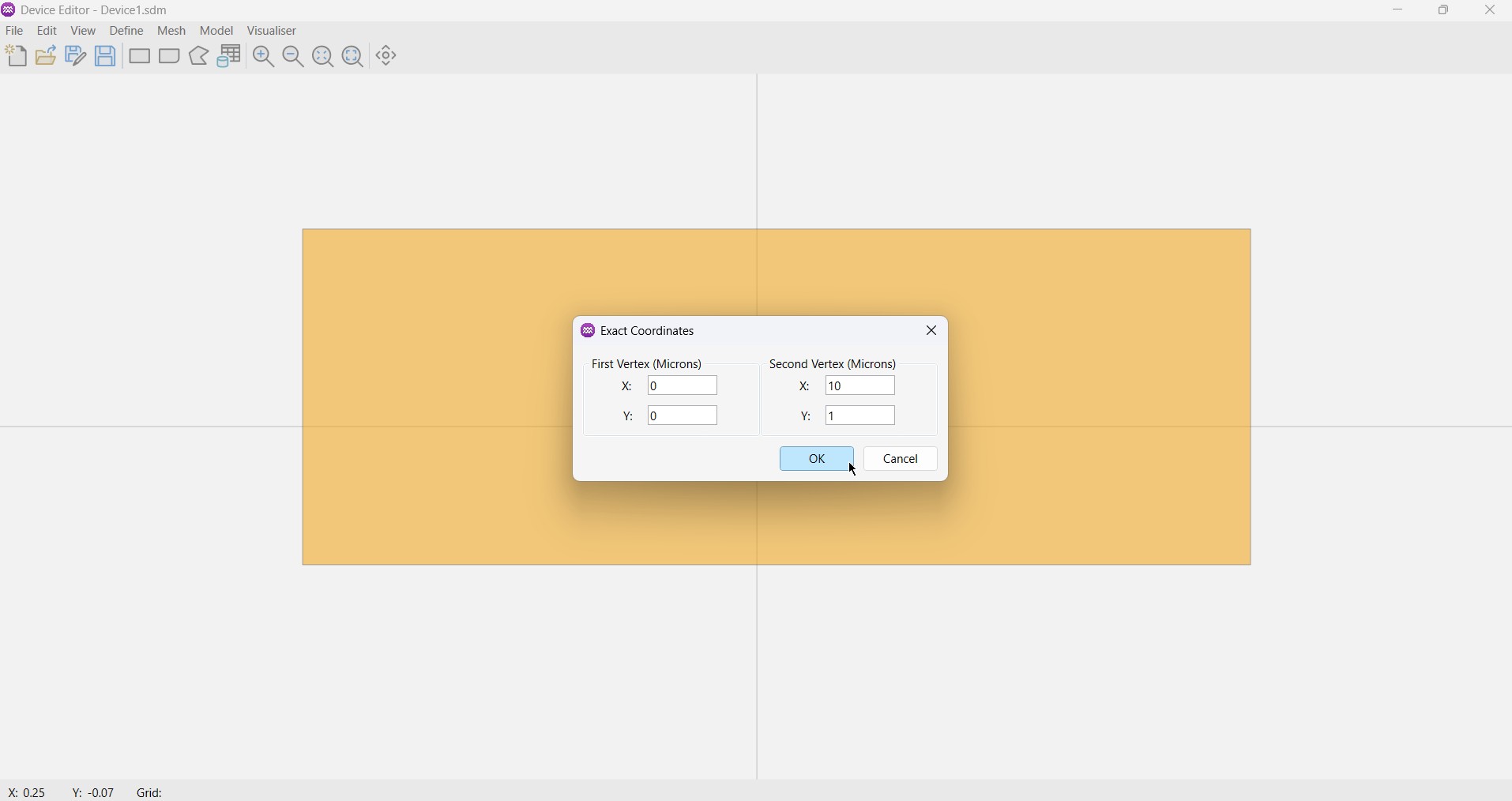
- After drawing the rectangle, the Exact Coordinates dialog will open automatically:
- Set the First Vertex to
(0, 0). - Set the Second Vertex to
(1, 10). - Click
OKto confirm.
- Set the First Vertex to
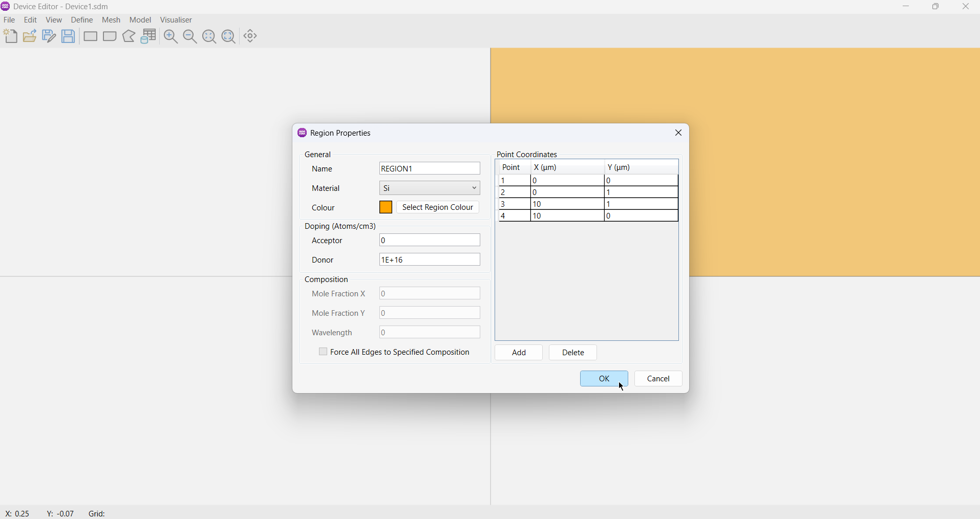
- The Region Properties dialog will then open:
- Set the Region Material to
Silicon (Si);- Note: the default material properties can be used, so the carrier mobility of
1000does not need to be changed.
- Note: the default material properties can be used, so the carrier mobility of
- Set the Donor Doping to
1E+16. - Click
OKto confirm.
- Set the Region Material to
For more detailed instructions on defining regions, click here.
4.1.3. Define the Device Contacts
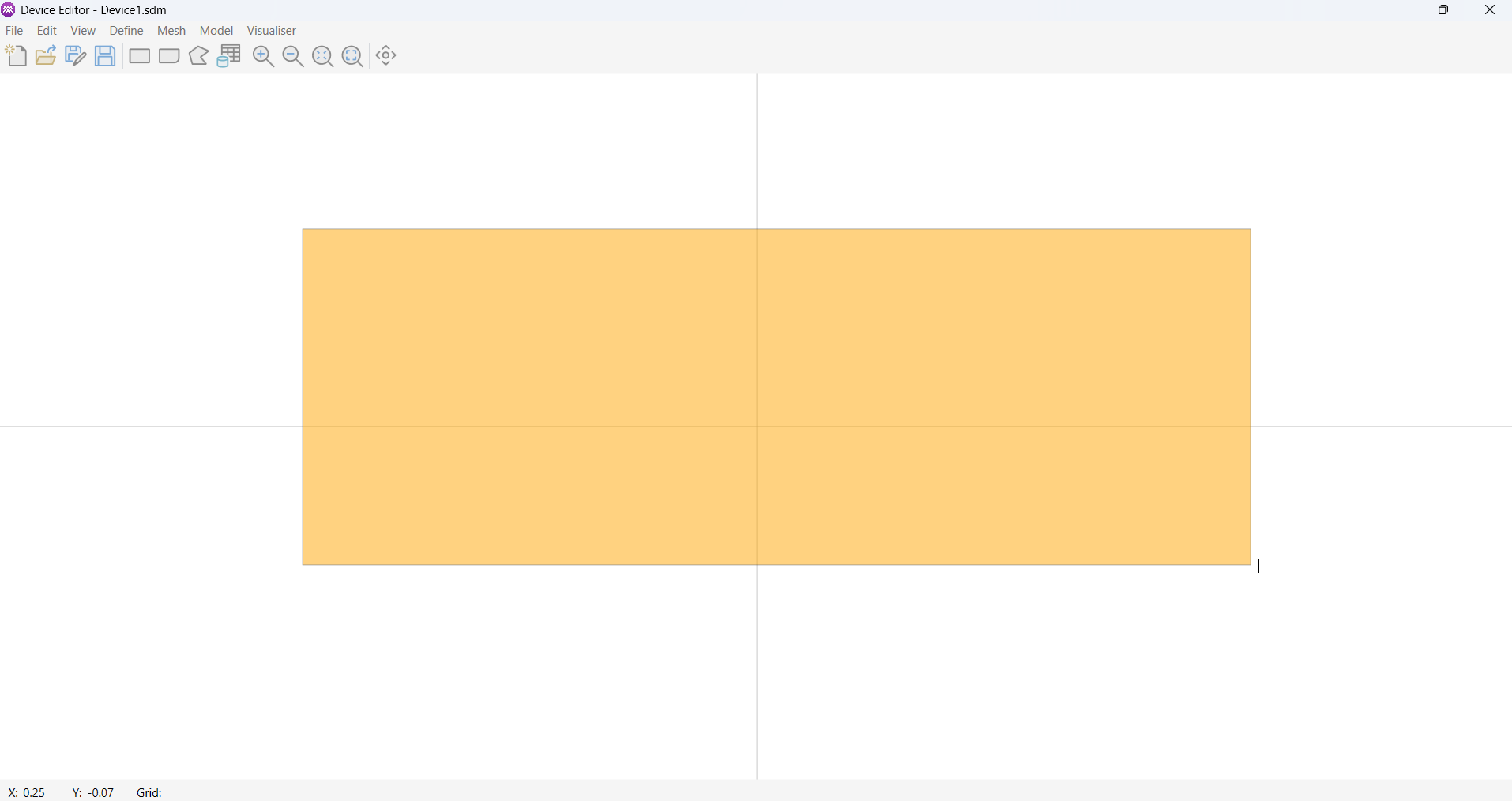
With the device geometry and material properties defined, the next step is to specify electrical contacts to allow the device to be connected to a circuit for simulation. In this example, the left and right edges of the region will be used to define contacts A and B, respectively, with the default contact parameters applied.
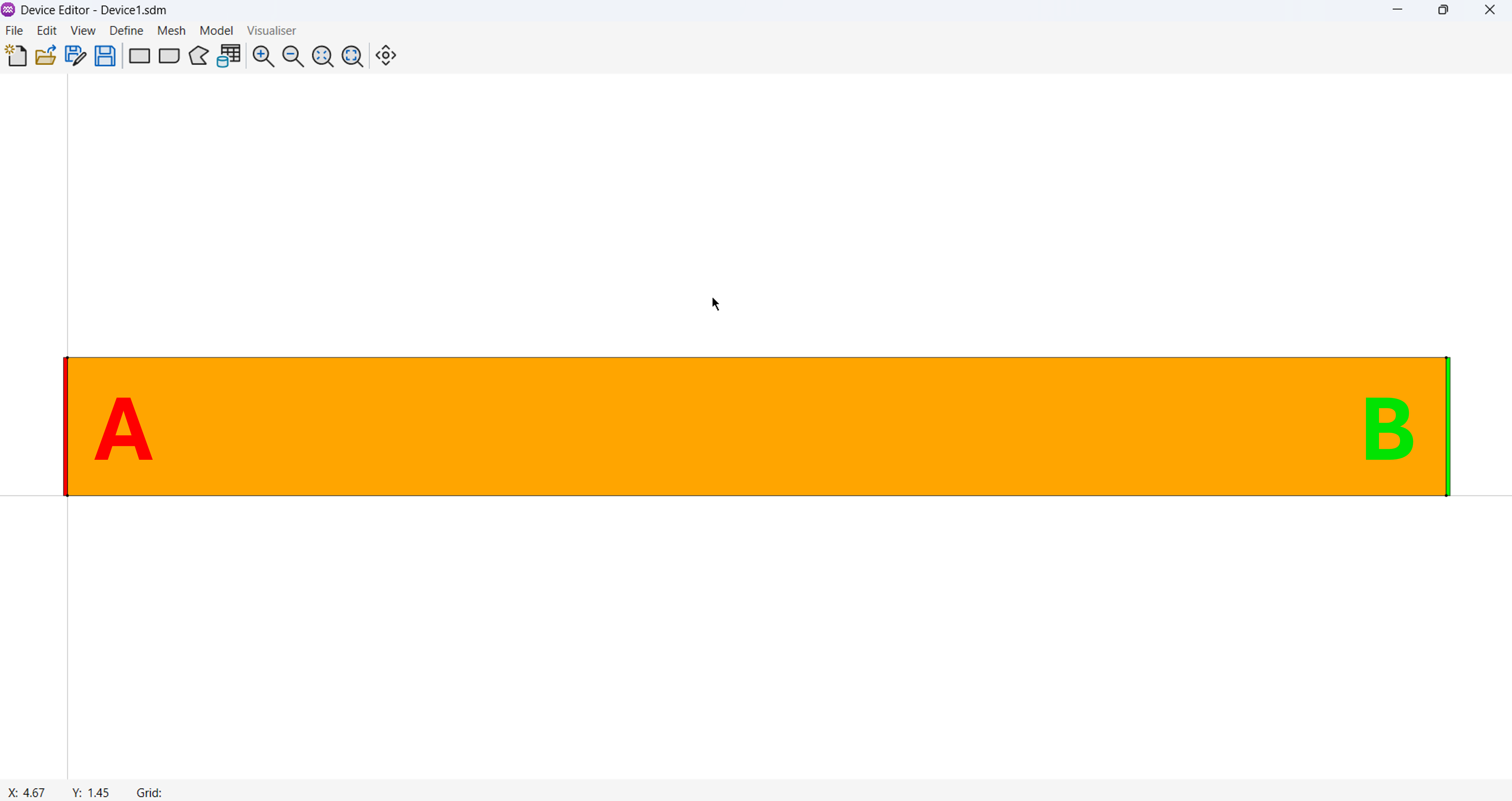
Define two contacts, A on the top of the device and B on the bottom as can been seen in the image above.
-
Define the first contact (A):
- From the menu, select
Define→Contact. - Move the cursor over the left geometric edge. When the edge highlights in green and the cursor changes to indicate a selectable element,
Left-clickto select it. Right-clickanywhere to open the Contact Properties dialog. Use this dialog to set the contact's properties.- In the General section, set
Nameto A, leave all other properties at their default values. - Click
OK.
- From the menu, select
-
Define the second contact (B), repeat steps 1–5 above, but instead:
- Select the bottom geometric edge.
- In the Contact Properties window, set
Nameto B andColourto green. - Click
OK.
For more detailed instructions on defining contacts, click here.
4.1.4. Define the Mesh Construction Lines
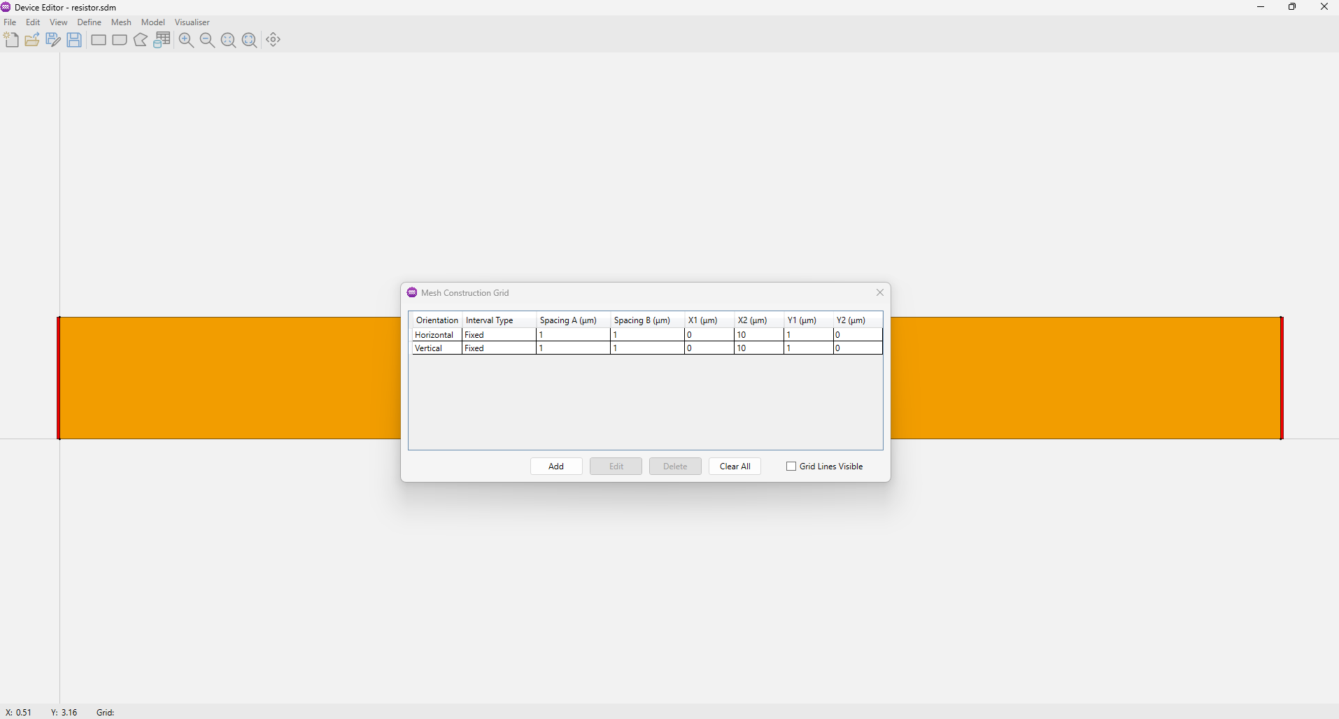
An initial grid is defined by specifying a set of vertical and horizontal lines. Anywhere these lines intersect with each other or with a region boundary, a point is inserted into the mesh.
For a simple resistor with uniform material properties and no junctions, a coarse mesh is sufficient. It provides a good balance between simulation accuracy and computational efficiency. Since the resistor is uniform along the x-direction (its properties do not change with x), we only need to define horizontal grid lines.
-
In the menu Menu Bar select
Mesh→Define Mesh Construction Grid. The Mesh Construction Grid window will open. -
In the Mesh Construction Grid window click
Add. -
The Mesh Grid Lines window will open. Set the below properties:
- Set the Orientation to
Horizontal. - Set the Interval to
Fixed. - Set the Coordinates of the box that will contain the mesh line to:
X1 = 0X2 = 1Y1 = 0Y2 = 10
- Set the Spacing Between Lines to
1.0microns.
- Set the Orientation to
-
Click
OK
For more detailed instructions on defining the mesh construction grid, click here.
4.1.5. Generating the Finite Element Mesh
- In the Menu Bar, select
Mesh→Generate Finite Element Mesh Model. The Mesh Properties window will open. - No refinement is required for this model, so click
OKto generate the mesh with default settings.
For more detailed instructions on generating the finite element mesh, click here.
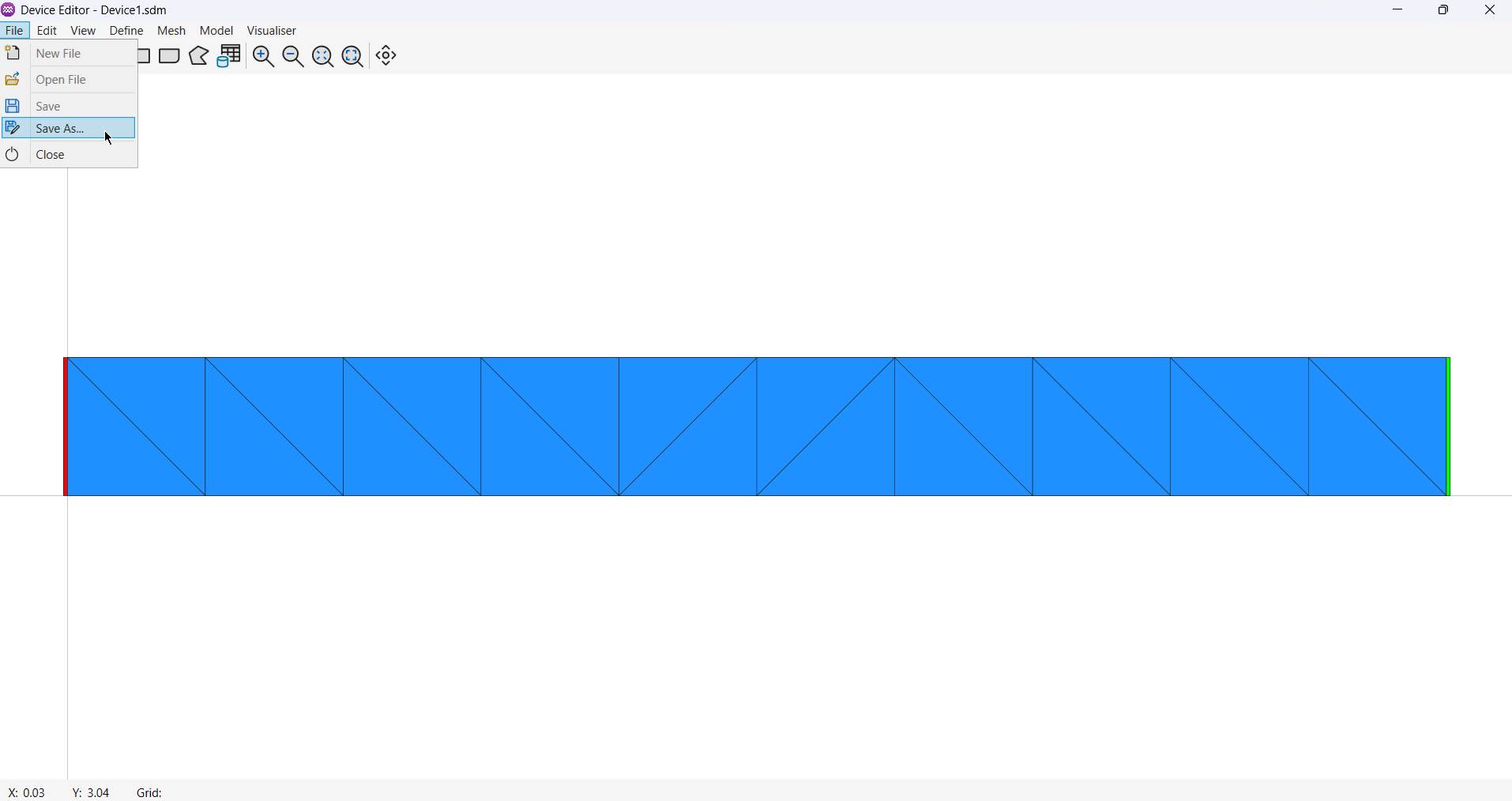
4.1.6. Save the Device Model
- In the Menu Bar, select
File→Save As.... The Save dialog will open. - Navigate to the folder you wish to save the device in.
- Specify the filename (e.g. resistor.sdm).
- Click
Saveto store the device model.
4.2. Steady State Simulation
Next the resistor will be used in a simple steady state example.
- On the Start Page Click New Simulation (the second option).
- The Circuit Editor will open with an empty workspace.
4.2.1. Simulation Setup
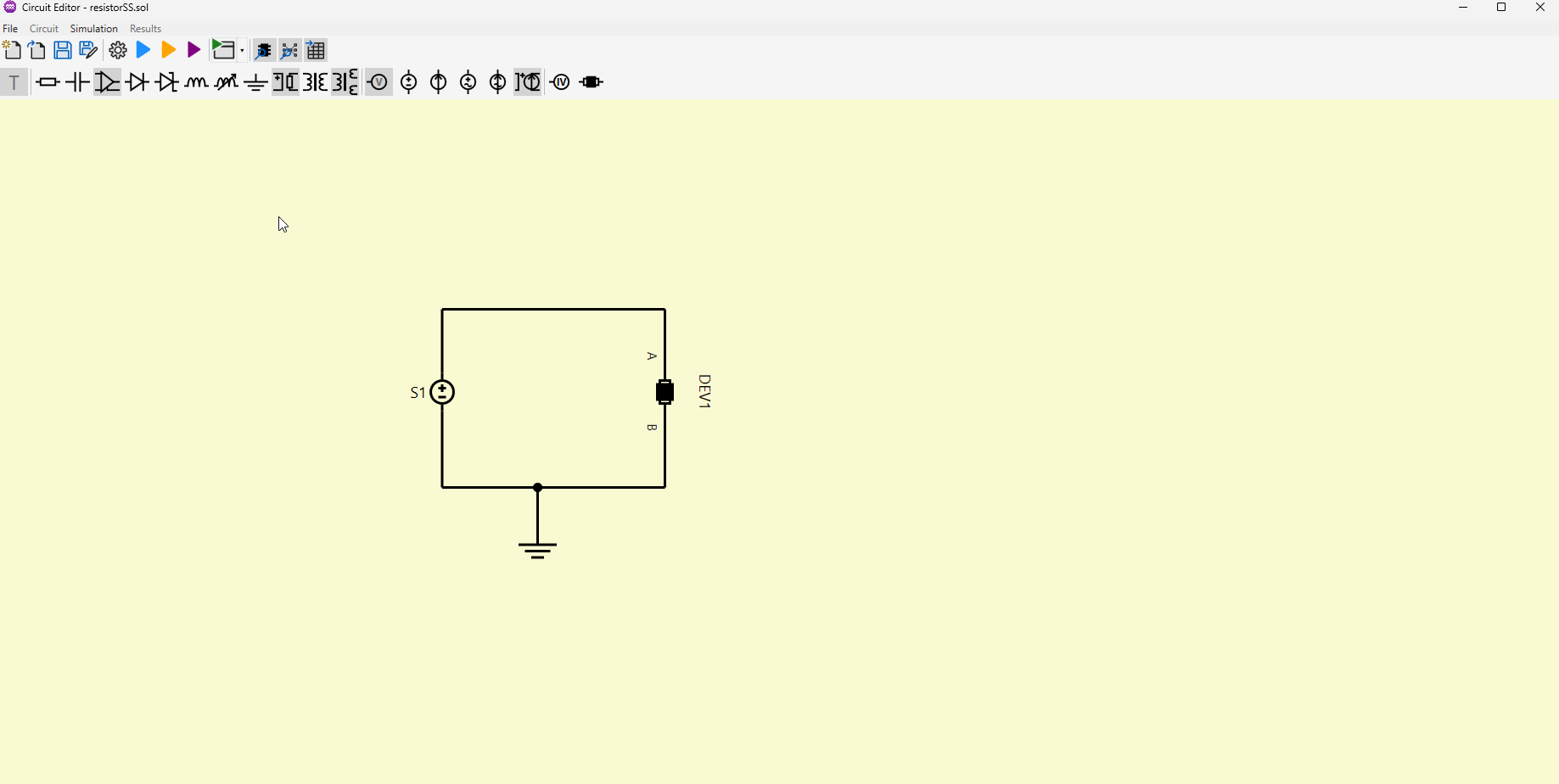
A circuit must be designed before simulation can begin. A device (the resistor), a DC Voltage Source and a Ground will be added to the circuit editor and connected together.
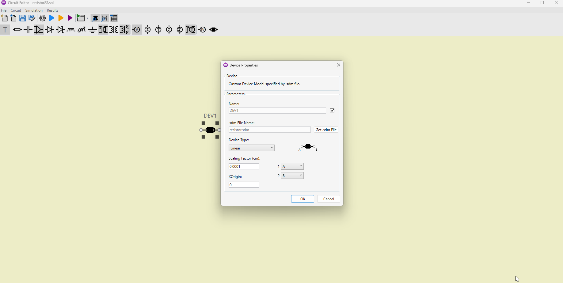
4.2.1.1. Add the Device
- Select the Device
 from the tool bar and drag and drop it onto the circuit editor.
 - Set the device Properties:
- Click
Get .sdm File, select the device file that you created in the previous steps and clickOK. - Ensure Scaling Factor (cm) is set to
0.0001. Which sets the device depth to 1m depth. - Click
OKto close the Device Properties.
- Click
Note: The device can be rotated by Left-clicking on it to select it and then using CTRL + R to rotate it by .
For more detailed instructions on Adding Components, click here.
4.2.1.2. Add a Source and Ground
- Select the DC Voltage Source
 from the tool bar by
 Dragging and Droppingit onto the circuit editor. - Select the Ground
 from the tool bar by
 Dragging and Droppingit onto the circuit editor. - Connect the components together as they are in the image below.
For more detailed instructions on Wiring Circuits, click here.
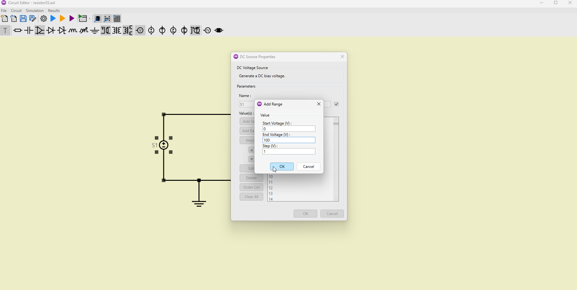
4.2.1.3. Set Source Properties
Double-clickon the DC Voltage Source to open its properties.- Click
Add Rangeto open the Add Range Properties and set to the values below:Start Voltage (V) = 0End Voltage (V) = 100Step (V) = 1- Click
OKto set the range.
- Click
OKto set the DC Voltage Source Properties.
For more detailed instructions on Steady State (DC) Sources, click here.
4.2.1.4. Save the Solution File
Save the simulation at this point.
- In the Menu Bar, select
File→Save As.... The Save dialog will open. - Navigate to the folder you wish to save the solution file.
- Specify the filename (e.g. resistor_iv.sol).
- Click
Saveto store the solution file.
4.2.2 Run Simulation
To run the Steady State Simulation press the blue run button![]() , alternatively in the menu use
, alternatively in the menu use Simulation → Steady State.
For more detailed instructions on Running a Simulations, click here.
The simulation will begin and the Simulation Status will appear on the screen. Wait until the simulation has completed at which point Simulation Stopped will appear in the bottom left of the status window and the text "Aquarius simulator completed execution." will be show in the screen.
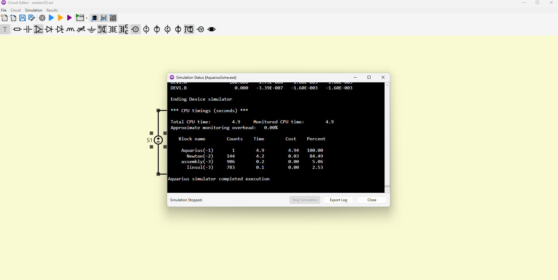
For more detailed instructions on the Simulation Status output, click here.
4.3. Simulation Results
4.3.1. Visualising the Results
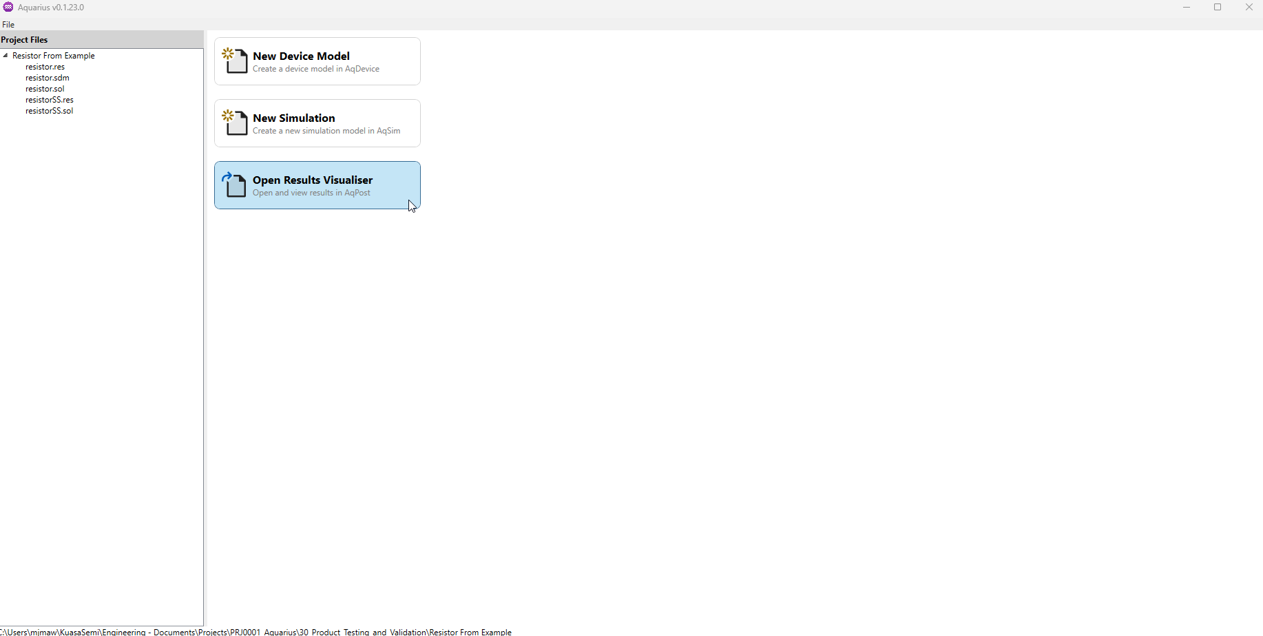
Next results visualiser will be used to understand the output of the simulation.
- On theStart Page Click
Open Results Visualiser(the third option). - The application will ask the user to select a
.resresults file.- The name of the
.resfile will be the same as the.solwhich has just run (e.g. resistor_iv.res).
- The name of the
- Then the Results Visualiser will open with the selected results file loaded.
- Click
External Plotat the top of the results visualiser. - Set External Plot Settings:
- The file should match your results file name.
X Axis Contact = DEV1.AX Axis Variable = VoltageY Axis Contact = DEV1.AX Axis Variable = Total Current- Click check box to turn on
Show Tick Marks
- Click
New Plotto generate a graph showing Total Current (A) at terminal A of DEV1 (the resistor's name) versus the Voltage (V) at the same terminal. The plot demonstrates a linear relationship between voltage and current, as expected.

4.3.2. Analysing the Results
Using Ohm's law the resistance through the device at a given voltage and current can be calculated. Taking the data point at 100V.
This matches the previously calculated resistance of , therefore the analytical model matches the TCAD simulation.
This concludes the Resistor example tutorial.
5. Conclusion
This example demonstrated how to model and simulate a simple uniformly doped silicon resistor in the Aquarius TCAD environment. The analytical resistance, derived from fundamental semiconductor relations, was shown to match the simulated result within numerical accuracy. This validates both the device modelling workflow and the simulator’s accuracy, while also serving as a clear instructional case for users learning to set up and analyse basic passive devices.