Contacts
1. Overview
Electrical, thermal and electrothermal contacts can be assigned to any edge (or combination of edges) along the perimeter of a region. A single contact may span multiple edges, and contacts can also be distributed across different regions, including junctions between regions. To successfully simulate a device, at least two contacts must be defined. A maximum of eight contacts can be added to a single device model.
2. Usage Instructions
To define a contact:
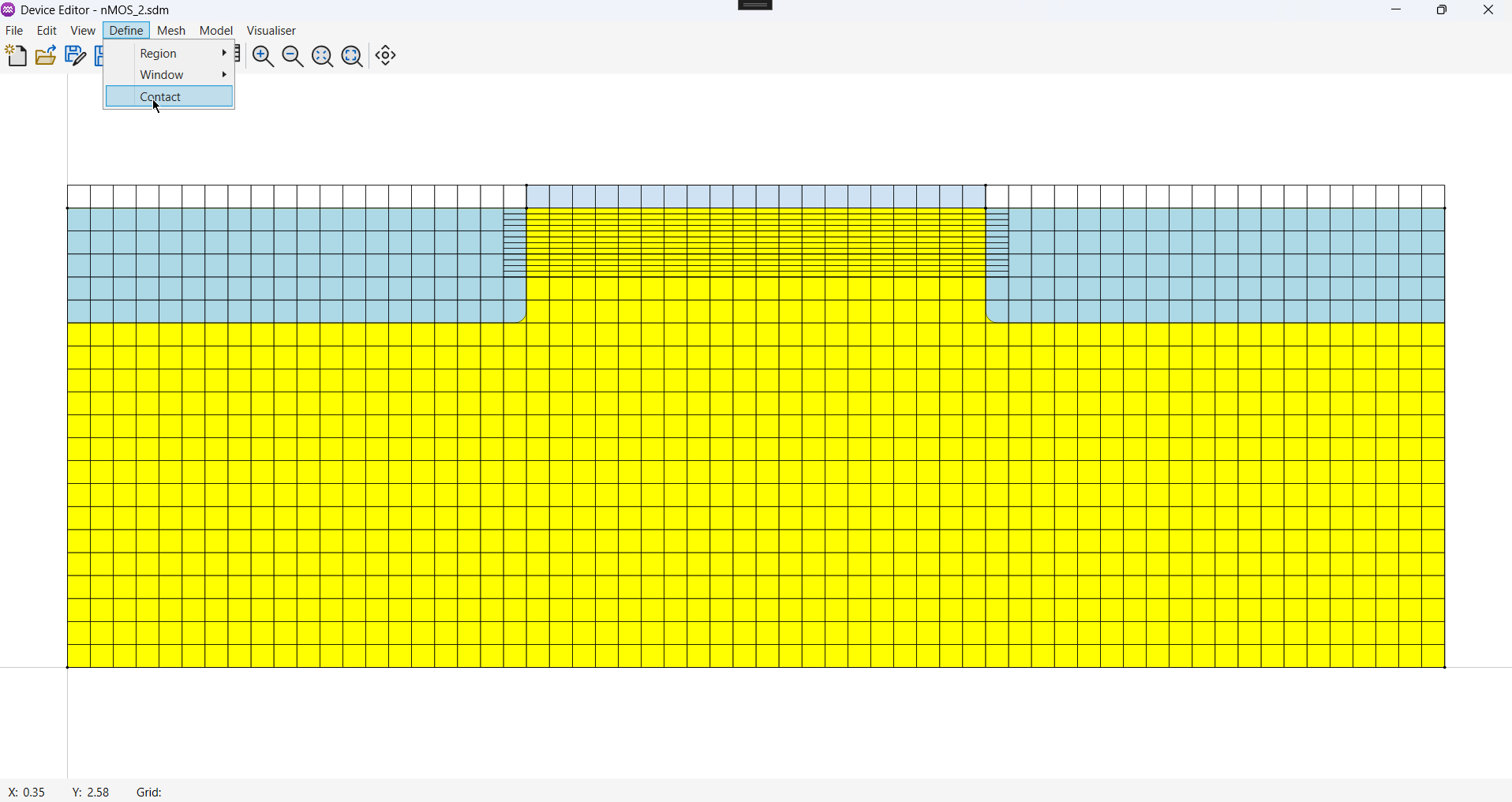
- From the Menu, select
Define→Contact.
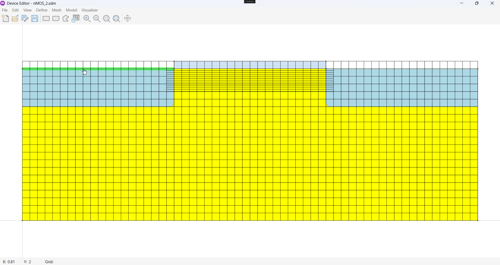
- Using the cursor, hover the cursor over the geometric edges that make up the contact. When the edge is highlighted in green and the cursor changes to indicate a selectable element, left-click to select the edge.
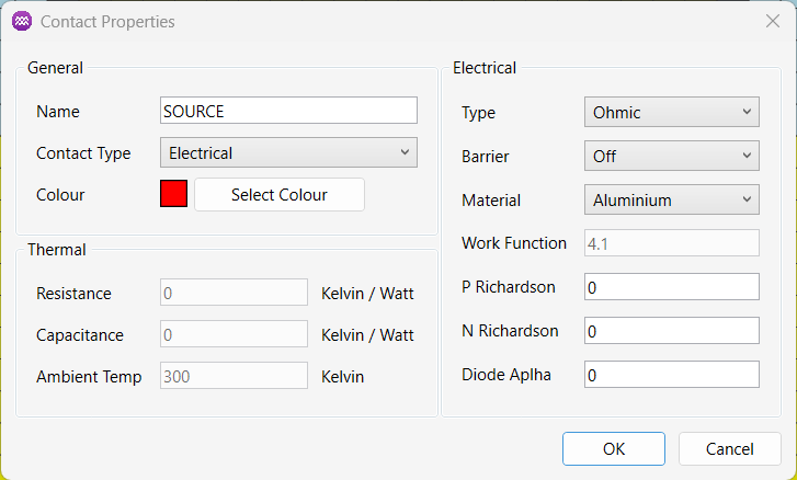
- After defining all the contact edges, right-click anywhere to open the properties dialog for the contact. Use this dialog to set the contact's properties.
3. Parameters
3.1. General
| Name | Description | Unit |
|---|---|---|
Name | A unique identifier for the contact. | - |
Type | Used to define how contact will interact with the semiconductor. Options: [Electrical, Thermal, Electro-thermal] | - |
Colour | Used to define visual colour of the contact (Not used in the solver). | - |
3.2. Thermal
| Name | Description | Unit |
|---|---|---|
Resistance | Used to define the thermal resistance. | K/W |
Capacitance | Used to define the thermal capacitance. | J/K |
Ambient Temperature | Used to define the ambient temperature used in the simulation. | K |
3.3. Electrical
| Name | Description | Unit |
|---|---|---|
Type | Used to define the electrical contact type Options: [Ohmic, Schottky] | - |
Material | Used to specify the material used for the contact. | - |
Work Function | Defines the work function of the contact material. This value is automatically filled in when you choose a predefined material. If the material you need is not listed, select “Other” and manually enter a custom value. | eV |
P Richardson | If set to a non-zero, the value is used as the Richardson constant to calculate the thermionic emission current for holes. See Thermionic Emission for details. | Acm-2K-2 |
N Richardson | If set to a non-zero, the value is used as the Richardson constant to calculate the thermionic emission current for electrons. See Thermionic Emission for details. | Acm-2K-2 |
Barrier Lowering | Enables or disables field‑induced barrier lowering. Used together with the dipole barrier‑lowering coefficient. See Barrier Lowering for details. [On, Off] | - |
Dipole Alpha | Coefficient used to calculate dipole‑induced barrier lowering at Schottky contacts. See Barrier Lowering for details. | cm |
3.3.1. Thermionic Emission
The thermionic emission current densities for electrons () and holes () are given by:
where:
- , = Richardson constants (holes and electrons) [Acm-2K-2]
- = Temperature [K]
- = Elementary charge [C]
- = Barrier height [eV]
- = Barrier height lowering [eV]
- = Boltzmann constant [eV/K]
3.3.2. Barrier Lowering
The total barrier lowering is given by:
where:
- = Total barrier lowering [eV]
- = Elementary charge [C]
- = Electric field at the interface [Vcm-1]
- = Permittivity of the semiconductor [Fcm-1]
- = Dipole lowering coefficient [cm]
The first term is Schottky barrier lowering, and the second term is dipole‑induced barrier lowering.
The dipole term typically corresponds to an effective dipole layer thickness < 2 nm.