Physical Models
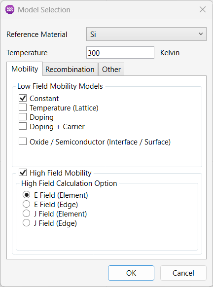
A range of physical models are available to be used in the simulation. The physical models implemented in the simulator are fully configurable. To edit or view the physical models properties:
- From the main menu, select
Model->Model Selection.
Parameters
1. General
| Name | Description | Unit |
|---|---|---|
Reference Material | The baseline material used to define reference energy levels in simulations. | - |
Temperature | Ambient temperature for the simulation. | K |
2. Mobility
The mobility is determined through a combination of physical effects that represent how different scattering mechanisms influence carrier transport. The calculation process is divided into two parts:
- Low Field
- High Field
The resulting low-field mobility is then used as an input to the high-field mobility calculation.
2.1. Low Field
Users can configure low-field mobility using different models:
- Constant Model: Mobility is fixed to the value specified in the properties command.
- Lattice (Temperature) Model: Mobility varies with temperature due to lattice scattering effects.
When using the Temperature (Lattice) Model, users can optionally include:
- Impurity Model: Accounts for mobility reduction caused by doping-related impurity scattering.
- Carrier-Carrier Model: Extends the impurity model by also considering carrier-carrier scattering, which becomes significant at high injection levels.
If the high-field model is selected, the low-field mobility model will feed into it. Otherwise, the selected mobility model will be used in the simulation.
2.1.1. Constant
This is the simplest form of mobility and simply sets the low-field mobility for each semiconductor material type to be constant.
where:
| Symbol | Description | Units | Property (holes) | Property (electrons) |
|---|---|---|---|---|
| Constant mobility. | cm2/Vs | MU_0_P | MU_0_N |
2.1.2. Lattice
The lattice mobility uses an empirical model to take into account the scattering that occurs between the lattice and the carriers contained in it. This is simply a function of lattice temperature (), increased temperature leads to a reduction in carrier mobility:
where:
| Symbol | Description | Units | Property (holes) | Property (electrons) |
|---|---|---|---|---|
| Mobility at the reference temperature. | cm2/Vs | MU_MAX_P | MU_MAX_N | |
| Temperature exponent, a material-specific empirical parameter. | - | MU_ALPT_P | MU_ALPT_N | |
| Lattice temperature. | K | - | - |
References
[1] J. Bardeen and W. Shockley, “Deformation potentials and mobilities in non‑polar crystals,” Physical Review, vol. 80, no. 1, pp. 72–80, 1950.
[2] S. M. Sze and K. K. Ng, Physics of Semiconductor Devices, 2nd ed. Hoboken, NJ, USA: Wiley, 1981, p. 28.
2.1.3. Impurity
The impurity (doping) mobility model expression is used to describe how carrier mobility decreases with increasing doping concentration. The model combines the lattice-limited mobility with impurity scattering effects, ensuring a smooth transition between low and high doping regions.
| Symbol | Description | Units | Property (holes) | Property (electrons) |
|---|---|---|---|---|
| Minimum mobility. | cm2/Vs | MU_MIN_P | MU_MIN_N | |
| Lattice limited (maximum) mobility. | cm2/Vs | - | - | |
| Temperature coefficient for lattice scattering mobility. | - | MU_ALPD_P | MU_ALPD_D | |
| Reference doping concentration. | cm-3 | MU_NREF_P | MU_NREF_N | |
| Acceptor concentration. | cm-3 | - | - | |
| Donor concentration. | cm-3 | - | - |
References
[1] D. M. Caughey and R. E. Thomas, “Carrier mobilities in silicon empirically related to doping and field,” Proceedings of the IEEE, vol. 55, no. 12, pp. 2192-2193, Dec. 1967.
2.1.4. Carrier-carrier
The carrier-carrier scattering mobility model extends the impurity mobility formulation by including the effect of carrier-carrier interactions under conditions of high injection. In this model, the mobility depends not only on the doping concentration but also on the total carrier concentration. The lattice-limited mobility again defines the maximum achievable mobility.
| Symbol | Description | Units | Property (holes) | Property (electrons) |
|---|---|---|---|---|
| Minimum mobility | cm2/Vs | MU_MIN_P | MU_MIN_N | |
| Temperature coefficient for lattice scattering mobility | - | MU_ALPD_P | MU_ALPD_D | |
| Reference doping concentration | cm-3 | MU_NREF_P | MU_NREF_N | |
| Lattice limited (maximum) mobility | cm2/Vs | - | - | |
| Acceptor concentration | cm-3 | - | - | |
| Donor concentration | cm-3 | - | - | |
| Electron concentration | cm-3 | - | - | |
| Hole concentration | cm-3 | - | - |
References
[1] H. Engl, R. Lindl, and C. Selberherr, “A physically based mobility model for numerical simulation of semiconductor devices,”IEEE Transactions on Computer-Aided Design of Integrated Circuits and Systems, vol. 7, no. 2, pp. 231–239, 1988.
2.2. Interface
This interface models are only calculated for element edges that lies on an oxide/semiconductor interface.
2.2.1. Surface Field-Dependant
This model accounts for the reduction of carrier mobility caused by the perpendicular electric field at an oxide/semiconductor interface. As the surface field increases, carriers experience enhanced surface scattering, which lowers their effective mobility. The strength of this degradation is controlled by the ratio of the perpendicular field to a critical field value, ensuring that mobility transitions smoothly from its low‑field value to a reduced high‑field value under strong surface electric fields.
| Symbol | Description | Units | Property (holes) | Property (electrons) |
|---|---|---|---|---|
| Oxide interface mobility reduction factor. | - | MU_GSUR_P | MU_GSUR_N | |
| Low field mobility value. | cm2/Vs | - | - | |
| The perpendicular electric field. | V/cm | - | - | |
| The critical electric field, at which mobility degradation becomes strong. | V/cm | MU_S_EC_P | MU_S_EC_N |
References
[1] T. Ando, A. B. Fowler, and F. Stern, “Electronic properties of two‑dimensional systems,” Reviews of Modern Physics, vol. 54, no. 2, pp. 437–672, Apr. 1982.
2.2.2. Lombardi Model
The Lombardi mobility model captures how multiple physical scattering mechanisms at the semiconductor/oxide interface degrade the effective carrier mobility. The total mobility is obtained by combining the individual scattering components using Matthiessen’s rule. Each mechanism contributes an additive inverse‑mobility term. The user can select to use surface roughness and acoustic or either on their own.
The full mobility expression is:
where:
| Symbol | Description | Units |
|---|---|---|
| Bulk mobility, this is calculated from the low-field model(s) that are selected. | cm2/Vs | |
| Acoustic‑scattering‑limited mobility. | cm2/Vs | |
| Surface‑roughness‑limited mobility. | cm2/Vs |
References
[1] C. Lombardi, S. Manzini, A. Saporito, and M. Vanzi, “A physically based mobility model for numerical simulation of nonplanar devices," IEEE Trans. Comput.-Aided Des. Integr. Circuits Syst., vol. 7, no. 11, pp. 1164–1171, 1988.
[2] A. Pérez‑Tomás, P. Brosselard, P. Godignon, J. Millán, N. Mestres, M. R. Jennings, J. A. Covington, and P. A. Mawby, “Field‑effect mobility temperature modeling of 4H‑SiC metal‑oxide-semiconductor transistors,” J. Appl. Phys., vol. 100, p. 114508, 2006.
The user can enable surface‑roughness scattering, acoustic scattering, or both together, with bulk mobility always included.
2.2.2.1. Acoustic Scattering
This term captures mobility loss due to acoustic phonon interaction enhanced by the vertical electric field.
where:
| Symbol | Description | Units | Property (holes) | Property (electrons) |
|---|---|---|---|---|
| Base acoustic‑scattering coefficient. | - | MU_LOMB_B_P | MU_LOMB_B_N | |
| Doping‑dependent acoustic‑scattering coefficient. | - | MU_LOMB_C_P | MU_LOMB_C_N | |
| The total ionised doping concentration (). | cm-3 | - | - | |
| Doping‑dependence exponent. | - | MU_LOMB_ALPHA_P | MU_LOMB_ALPHA_N | |
| The perpendicular electric field. | V/cm | - | - | |
| Field‑dependence exponent for first term. | - | MU_LOMB_BETA_P | MU_LOMB_BETA_N | |
| Lattice temperature. | K | - | - | |
| Field‑dependence exponent for second term. | V/cm | MU_LOMB_GAMMA_P | MU_LOMB_GAMMA_N |
2.2.2.2. Surface Roughness Scattering
Surface roughness increases carriers' interaction with the oxide boundary when the perpendicular electric field becomes large.
where:
| Symbol | Description | Units | Property (holes) | Property (electrons) |
|---|---|---|---|---|
| Surface‑roughness scattering coefficient. | - | MU_LOMB_A_P | MU_LOMB_A_N | |
| The perpendicular electric field. | V/cm | - | - | |
| Field‑dependence exponent. | - | MU_LOMB_DELTA_P | MU_LOMB_DELTA_N |
2.3. High Field
The high-field mobility reduction describes the effect of velocity saturation at high fields. This is applied after the low-field mobility has been calculated, thus uses the resultant value of low field mobility described above.
The user can choose how the high field is evaluated and how it is calculated across the mesh.
There are two options to selects which quantity is used to determine the high-field mobility reduction:
- E Field: The high field is taken as the magnitude of the electric field.
- J Field: The high field is taken as the component of the electric field in the direction of the current (useful when current flow direction is important).
There are also two options to specify how the high field is computed spatially:
- Edge: The high field is calculated using values along the edges of each mesh element.
- Element: The high field is calculated using values averaged over the entire element.
Together, these settings determine both what defines the high field and how that field is obtained during the mobility calculation.
| Name | Description | Unit |
|---|---|---|
E_MOB | Enables high-field mobility using the electric field magnitude, with the high field averaged over the entire mesh element.Options: [On, Off] | - |
E_EDG_MOB | Enables high-field mobility using the electric field magnitude, evaluated along the edges of each mesh element. Options: [On, Off] | - |
J_MOB | Enables high-field mobility using the component of the electric field in the direction of the current, with the high field averaged over the entire mesh element. Options: [On, Off] | - |
J_EDG_MOB | Enables high-field mobility using the component of the electric field in the direction of the current, evaluated along the edges of each mesh element. Options: [On, Off] | - |
Only one of these options can be on, default is all off.
The field dependency is implemented using the following expressions for the saturation velocity and mobility.
2.3.1. Saturation Velocity
| Symbol | Description | Units | Property (holes) | Property (electrons) |
|---|---|---|---|---|
| Saturation velocity at the reference temperature. | cm/s | MU_VSAT_P | MU_VSAT_N | |
| Temperature exponent. | - | VS_COEFTP | VS_COEFTN |
References
[1] C. Canali, G. Ottaviani, and A. Alberigi‑Quaranta, “Drift velocity of electrons and holes and associated anisotropic effects in silicon,” J. Phys. Chem. Solids, vol. 32, no. 8, pp. 1707–1720, 1971.
[2] S. Takagi, A. Toriumi, et al., “On the Universality of Inversion Layer Mobility in Si MOSFETs,” IEEE Transactions on Electron Devices, vol. 41, no. 12, pp. 2357–2362, Dec 1994.
2.3.2. Mobility
| Symbol | Description | Units | Property (holes) | Property (electrons) |
|---|---|---|---|---|
| Low field mobility. | cm2/Vs | - | - | |
| Saturation velocity at the reference temperature. | cm/s | - | - | |
| Electric field. | V/cm | - | - | |
| Empirical fitting parameter. | - | MU_BETA_P | MU_BETA_N |
References
[1] D. M. Caughey and R. E. Thomas, “Carrier mobilities in silicon empirically related to doping and field,” Proc. IEEE, vol. 55, no. 12, pp. 2192–2193, Dec. 1967.
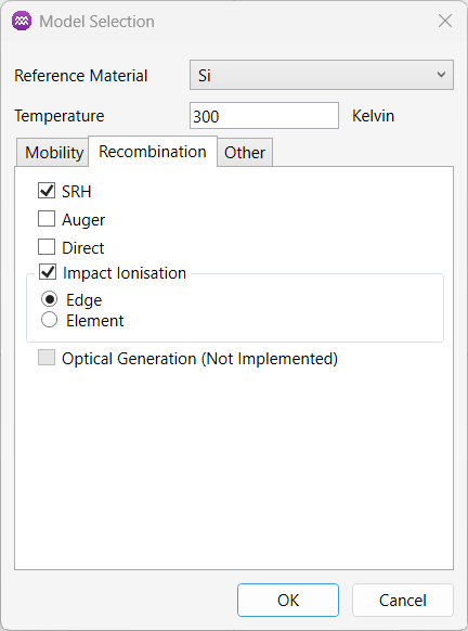
3. Recombination
This section describes the recombination models implemented in Aquarius. Each model is defined independently. Although the mechanisms can interact, these interactions are automatically managed by the solver.
3.1. Shockley-Read-Hall (SRH)
This model describes trap-assisted recombination occurring within the bulk of the semiconductor, based on the Shockley–Read–Hall (SRH) mechanism. It accounts for the dependence of minority carrier lifetime on doping concentration, allowing accurate modelling of recombination in heavily doped regions. Additionally, the position of the trap energy level within the bandgap is adjustable, enabling flexibility to represent different defect states. Users can define up to 10 trap levels, and the total SRH recombination is calculated as the sum of all defined levels. The model is defined by:
where:
| Symbol | Description | Units | Property |
|---|---|---|---|
| Electron concentration. | cm-3 | - | |
| Hole concentration. | cm-3 | - | |
| Intrinsic carrier concentration. | cm-3 | - | |
| , | Doping dependent carrier lifetimes. | s | - |
| Trap energy level relative to intrinsic level. | eV | E_TRAP | |
| Boltzmann constant. | eV/K | - | |
| Absolute temperature. | K | - |
The doping dependent lifetimes, and , are defined by:
where:
| Symbol | Description | Units | Property (holes) | Property (electrons) |
|---|---|---|---|---|
| Acceptor doping concentration. | cm-3 | - | - | |
| Donor doping concentration. | cm-3 | - | - | |
| Reference doping concentration. | cm-3 | - | - | |
| Reference carrier lifetime. | s | SRH_TAU_P | SRH_TAU_N | |
| Empirical fitting parameter. | - | SRH_AP | SRH_AN | |
| Empirical fitting parameter. | - | SRH_BP | SRH_BN | |
| Empirical fitting parameter. | - | SRH_CP | SRH_CN | |
| Empirical fitting parameter. | - | SRH_DP | SRH_DN |
Additionally, the carrier lifetime can be made position-dependent by applying a scaling factor within a defined rectangular region of the device. This is achieved using an SRH Window, which specifies a box in the device model where the carrier lifetimes in the bulk are multiplied by a user-defined factor. This feature allows localised adjustment of recombination properties to model non-uniform defect distributions or process-induced variations.
3.2. Auger
The Auger mechanism becomes the dominant recombination process under conditions of high carrier injection, such as in heavily forward-biased regions or during high-level injection in power devices. It involves a three-particle interaction where the recombination energy is transferred to a third carrier instead of being emitted as a photon. It is modelled using:
where:
| Symbol | Description | Units | Property |
|---|---|---|---|
| Electron concentration. | cm-3 | - | |
| Hole concentration. | cm-3 | - | |
| Intrinsic carrier concentration. | cm-3 | - | |
| Auger coefficient for holes. | cm6s-1 | AUGER_CP | |
| Auger coefficient for electrons. | cm6s-1 | AUGER_CN |
3.3. Direct
The Direct recombination mechanism models band-to-band recombination, where an electron directly recombines with a hole without involving a trap state.
where:
| Symbol | Description | Units | Property |
|---|---|---|---|
| Electron concentration. | cm-3 | - | |
| Hole concentration. | cm-3 | - | |
| Intrinsic carrier concentration. | cm-3 | - | |
| Direct recombination coefficient. | cm-3s-1 | DIRECT_C |
3.4. Total Recombination Rate
The total recombination rate is found by summing up all the different mechanisms.
4. Generation
4.1. Impact Ionisation
The net impact ionization generation rate
where:
- = electron ionisation coefficient (cm-1)
- = hole ionisation coefficient (cm-1)
- = electron current density (A/cm2)
- = hole current density (A/cm2)
- = elementary charge (C)
There are two models for available impact ionisation, Chynoweth and Okuto-Crowell. Users can also select two options for the discretisation element or edge.
| Name | Description | Unit |
|---|---|---|
Chynoweth (Edge) | Selects the Chynoweth impact-ionisation model using full elemental discretisation. Options: [On, Off] | - |
Chynoweth (Element) | Selects the Chynoweth impact-ionisation model based on edge discretisation. Options: [On, Off] | - |
Okuto-Crowell (Element) | Selects the Okuto-Crowell impact-ionisation model using full elemental discretisation. Options: [On, Off] | - |
Okuto-Crowell (Edge) | Selects the Okuto-Crowell impact-ionisation model based on edge discretisation. Options: [On, Off] | - |
Only one option can be selected at any time. Default is all off.
For more details on the calculation types see Edge‑Based vs. Element‑Based Calculation of Vector Quantities.
4.1.1. Chynoweth
This law, developed by A. G. Chynoweth based on experimental work, provides an empirical relationship for the ionisation coefficient () as a function of the electric field ().
where:
| Symbol | Description | Units | Property (holes) | Property (electrons) |
|---|---|---|---|---|
| Ionisation coefficient prefactor | cm⁻¹ | AV_ALPH_P | AV_ALPH_N | |
| Field scaling parameter | V/cm | AV_BETA_P | AV_BETA_N | |
| Electric field | V/cm | - | - |
References
[1] A. G. Chynoweth, “Ionization rates for electrons and holes in silicon,” Phys. Rev., vol. 109, no. 5, pp. 1537-1540, Sep. 1958.
4.1.2. Okuto-Crowell
The Okuto-Crowell model extends the Chynoweth model by adding temperature and field dependence, providing a more accurate description of impact ionisation under varying thermal and electric field conditions.
where:
| Symbol | Description | Units | Property (holes) | Property (electrons) |
|---|---|---|---|---|
| Pre-exponential factor | cm⁻¹ | OC_A_P | OC_A_P | |
| Field scaling parameter | V/cm | OC_B_P | OC_B_N | |
| Temperature coefficient (prefactor) | 1/K | OC_C_P | OC_C_N | |
| Temperature coefficient (field scaling) | 1/K | OC_D_P | OC_D_N | |
| Exponent in exponential term | - | OC_M_P | OC_M_N | |
| Field-power exponent | - | OC_N_P | OC_N_N | |
| Electric field | V/cm | - | - | |
| Lattice temperature | K | - | - |
References
[1] Y. Okuto and C. R. Crowell, "Ionization coefficients in semiconductors: A nonlocalized property," Phys. Rev. B, vol. 10, no 10, pp. 4284-4296, 1974, doi:10.1103/PhysRevB.10.4284.
4.2. Constant Generation
When enabled, constant generation applies a uniform carrier generation rate within one or more specified regions of the device. Users can choose to:
- Apply the same constant generation rate across all semiconductor regions of the device, or
- Assign specific generation rates to individual regions for more localised control.
4.3. Total Generation
The total generation rate is found by summing up all the different mechanisms.
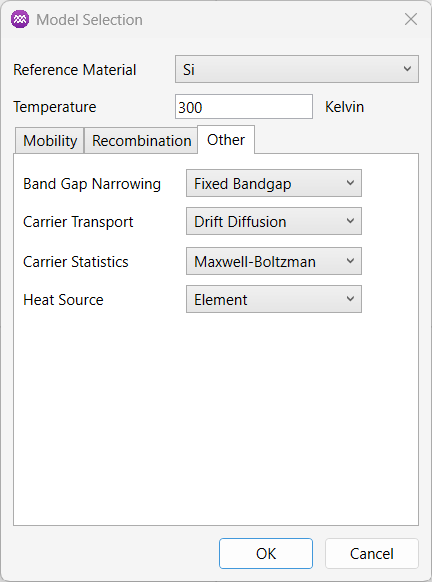
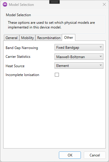
5. Other
5.1. Bandgap Narrowing
Bandgap narrowing occurs in heavily doped regions of the semiconductor, where the impurity bands merge into either the conduction band or valence band, effectively reducing the bandgap.
The reduction in the intrinsic bandgap is defined as:
The conduction band edge () and the valence band edge () shift relative to their intrinsic values ( and ) by half of the total narrowing, .
The conduction band edge () shifts downwards.
The valence band edge () shifts upwards.
And the electron affinity () as:
In Aquarius these models are only used for Silicon. For wide bandgap materials like Silicon Carbide (SiC) or Gallium Nitride (GaN), BGN is experimentally negligible, therefore these models do not apply and attempts to enable them are ignored.
Bandgap narrowing is accounted for using the following empirical models.
5.1.1. Slotboom's Model
Slotboom’s bandgap-narrowing model provides an empirical expression for how the semiconductor bandgap shrinks at very high doping levels by relating the reduction in bandgap to the logarithm of the total active dopant concentration.
where:
| Symbol | Description | Unit | Value |
|---|---|---|---|
| Bandgap narrowing. | eV | - | |
| Empirical fitting parameter. | eV | ||
| Absolute net doping concentration . | cm-3 | - | |
| Reference doping concentration. | cm-3 |
References
[1] J. W. Slotboom and H. C. de Graaff, “Measurements of bandgap narrowing in Si bipolar transistors,” Solid-State Electron., vol. 19, pp. 857-862, 1976.
5.1.2. Gaur's Model
Gaur’s bandgap-narrowing model offers a physically grounded framework for quantifying bandgap reduction in heavily doped semiconductors by analytically modelling the individual shifts in conduction and valence band edges as functions of dopant type and concentration.
where:
| Symbol | Description | Unit | Value |
|---|---|---|---|
| Bandgap narrowing. | eV | - | |
| Boltzmann constant (8.617333262×10⁻⁵) | eV/K | - | |
| Temperature. | K | - | |
| Absolute net doping concentration . | cm-3 | - |
The constants 1.52, 9.248×10⁻¹⁰, and the exponent 0.4678 come directly from empirical curve-fitting performed by Gaur et al. on experimentally measured bandgap narrowing data for heavily doped silicon.
References
[1] S. N. Gaur, “Band Gap Narrowing in Heavily Doped Silicon,” Solid-State Electronics, vol. 24, no. 11, pp. 1087-1089, 1981.
5.2. Carrier Statistics
Carrier concentrations in Aquarius are computed from the occupancy of states in the conduction and valence bands. Users may select between:
- Fermi-Dirac
- Maxwell-Boltzmann
The equations below follow the standard forms used in semiconductor physics.
Electrons in the Conduction Band:
- The full expression using corresponds to Fermi-Dirac statistics.
- The exponential approximation corresponds to Maxwell-Boltzmann statistics.
Holes in the Valence Band:
- Again, the Fermi-Dirac form uses the integral.
- The exponential form is the Maxwell-Boltzmann approximation.
Use the full Fermi-Dirac formulas when:
- Doping is degenerate (Fermi level close to a band edge).
- or lies within a few of or .
- Low‑temperature or high‑injection conditions are important.
Fermi-Dirac statistics correctly include the Pauli exclusion principle and remain accurate under strong degeneracy.
Use the Maxwell-Boltzmann exponential approximation when:
- The semiconductor is non‑degenerate.
- The quasi‑Fermi levels are more than 3-4 from the band edges.
- Faster simulation and reduced numerical cost are desired.
Maxwell-Boltzmann statistics are accurate for most moderately doped devices.
References
[1] Blakemore, J.S. Semiconductor Statistics. Dover Publications, New York, 1987. ISBN: 0‑486‑65383‑3
5.3. Heat Source
This setting specifies how the simulator computes the Joule heating term in the heat equation. Joule heating can be evaluated using element-based or edge-based calculations.
- Element
- The Joule heating source is calculated at the element level using element-averaged current densities and electric fields.
- Edge
- The Joule heating source is computed at the mesh-edge level, using edge-based current densities.
For more details on the calculation types see Edge‑Based vs. Element‑Based Calculation of Vector Quantities.
5.4. Incomplete Ionisation
Incomplete ionisation occurs when not all dopant atoms in a semiconductor contribute free charge carriers, typically due to insufficient thermal energy at low temperatures. This results in a carrier concentration lower than the physical doping level. While dopants are often assumed to be fully ionised, they occupy discrete energy levels within the bandgap. Ionisation depends on the Fermi level position and thermal energy ():
- At low temperatures, limited thermal energy leaves many dopants neutral, reducing free carriers compared to the doping concentration ( or ).
- At higher temperatures, more dopants ionise, approaching full activation.
Incomplete ionisation is significant in:
- Cryogenic conditions (freeze-out region)
- Materials with deep impurity levels
- High doping concentrations where the Fermi level shifts
Accurate device simulation, especially for SiC power devices across wide temperature ranges, requires accounting for incomplete ionisation to predict carrier concentrations, built-in potentials, and band bending.
The electrically active dopant concentration is determined using Fermi-Dirac statistics and depends on:
- Dopant energy depths.
- (donor to conduction band)
- (acceptor to valence band)
- Degeneracy factors ().
- Number of quantum states at impurity levels, influencing ionisation probability.
The fraction of ionised dopants is calculated as:
where:
| Symbol | Description | Units | Property |
|---|---|---|---|
| Number of ionised donors. | cm⁻3 | - | |
| Number of ionised acceptors. | cm⁻3 | - | |
| Number of donor impurities. | cm⁻3 | - | |
| Number of acceptor impurities. | cm⁻3 | - | |
| Donor degeneracy factor. | - | INCOMP_GD | |
| Acceptor degeneracy factor. | - | INCOMP_GA | |
| Donor ionisation depth. | eV | INCOMP_ED | |
| Acceptor degeneracy depth. | eV | INCOMP_EA | |
| Boltzmann constant (8.617333262×10⁻⁵). | eV/K | - | |
| Lattice temperature | K | - |
6. Edge‑Based vs. Element‑Based Calculation of Vector Quantities
Many TCAD models require evaluating vector quantities over the mesh. Aquarius offers two numerical approaches, edge‑based and element-based calculation, both aim to represent the same physical quantity but differ in how they interpret the underlying mesh data.
6.1. Edge‑Based Calculation
The quantity is evaluated on the mesh edges. Each edge connects two nodes, so the solver uses node‑to‑node differences to derive the vector quantity along that edge. These edge values are then distributed to the surrounding elements or used directly in edge‑based models.
Benefits:
- Very stable in regions with strong gradients, sharp junctions, or high‑field effects.
- Naturally consistent with discrete transport schemes.
- Preferred when robustness is more important than smoothness.
Limitations:
- The resulting field is defined only along edges, so it can appear less smooth.
- May require averaging or reconstruction to obtain element‑level quantities.
6.2. Element‑Based Calculation
The quantity is evaluated inside each element, using gradients reconstructed from the element's shape functions. Node values are interpolated across the element to form a continuous field. Gradients and vector quantities are computed directly within the element volume. This yields an element‑wide, volumetric representation of the vector field.
Benefits:
- Produces a smooth, continuous field across the domain.
- Often beneficial for coarse meshes or when thermal/electrical coupling requires smoothness.
- Compatible with fully FEM‑based formulations.
Limitations:
- Reconstructed fields can be less accurate when gradients are extremely steep.
- Can be less robust if the mesh is highly irregular or strongly anisotropic.
6.3. Summary
Use edge‑based when gradients are large, fields are steep, or the underlying transport equations use edge‑based fluxes (impact ionisation in avalanche regions, high‑field channels, power devices). Use element‑base when you want smoother spatial fields, stable coupling with thermal/mechanical solvers, or are working with coarse or uniform meshes.